Services and Engineering: II
UV-Lithography service:
This service comes as a package consisting of:
mask-engineering and manufacturing
resist-coating and softbake
exposure, development
final inspection
We have extensive knowledge in photoresist-processing and it starts with mask-engineering, substrate processing and ends with inspection of the patterned substrates.
We have identified our photoresist-processes as a very precious asset and constantly keep improving it.
New resists are being tested in collaboration with manufacturers of photochemicals. This allows us to be at the forefront of new photochemical developments.
We also take great precaution on particle contamination and are well equipped and trained to deliver high-quality patterned wafers, glass-plates and other customer substrates.
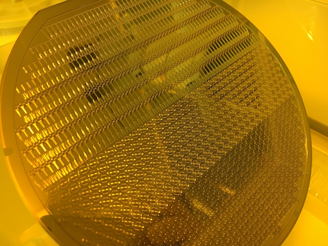
1: Processed wafer with 500µm SU-8, ready for electroforming
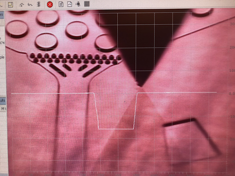
2: Profilometer-scan of a developed microfluidic-pattern
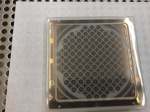
3: 5inch mask ready for production

4: 7 inch mask loaded into maskaligner
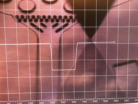
5: Profilometer-scan of a developed microfluidic-pattern
Specifications:
List standard available photoresists:
Various positive-tone Merck AZ resists for the full range of thicknesses.
Megaposit SPR 220 series
Kayaku (former: MicroChem) Photoexpoxy SU-8, KMPR
Image reversal Lift-off (AZ nLOF 20xx, TI35 ES, TI35 ESX)
=» Choice of appropriate auxillery chemicals (e.g. Thinner, Developer, EBR, Remover)
Substrate formats:
Round substrates: ø100, ø150, ø200, ø300mm
Square substrates: 4", 5", 6", 7", 9",10"
Available Resist thickness:
Positive-tone resists: 100nm - 80µm (e.g. AZ resists)
Negative-tone resists: 3µm - 550µm (e.g. SU-8)
Pattern resolution and innovation:
Minimal lateral feature size = 2µm
Overlay acccuracy depending on resist-thickness. @ Thin resist: 1-1.5µm
Aspect ratio = 5 - 6 (AR: pattern height / smallest footprint feature)
Our speciality: modifiying pattern to become transferred into resist optimal
Process flexibility:
Other resists, substrate formats or resist thicknesses on request.
1. Customer sends pattern-design (CAD-file, sketch,...)
2. applied microSWISS takes care of maskset-manufacturing
3. applied microSWISS to order appropriate substrates
4. Inspection and preparation of substrates (cleaning + adhesion promotor)
5. Resist coating and softbake with superior uniformity
6. UV-exposure, development and inspection of pattern
7. Packaging processed wafers in opaque container
8. Shipping with appropriate remarks for handling, care and storage