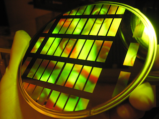
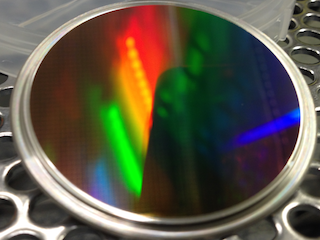
Hot-embossing stamps
Characteristics:
Master with a thickness range 0.5 - 3mm are being used on hot-embossing machines. Preferably called “stamp " The stamp is being screwed tightly to either heated base plate. An excellent physical contact between hotplate and stamp is vital to ensure proper thermal coupling.
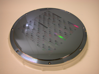
1: Hot-embossing stamp with sub-micro features and antisticking coating
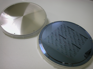
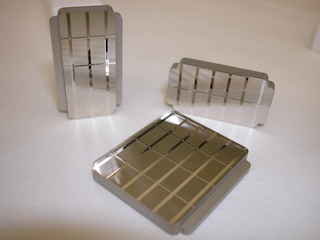
2: Hot-embossing stamps (front- and backside) with sub-micro features and antisticking coating.
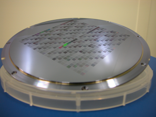
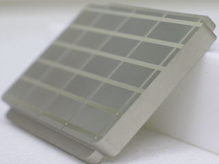
3: Hot-embossing stamps (frontside) with sub-micro features and antisticking coating.
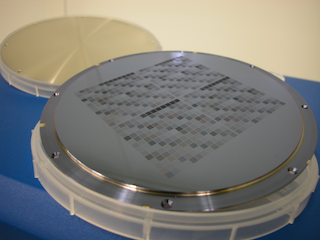
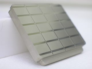
4: Hot-embossing stamps (front and backside) with sub-micro features and antisticking coating
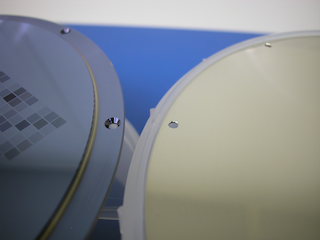
5: Mounting features and recess to fit EVG-machine
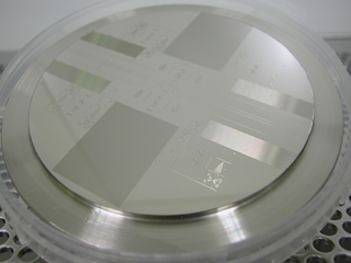
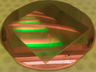
6: Hot-embossing stamp with various test features
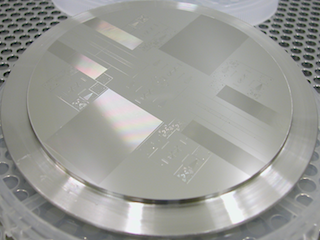
7: Hot-embossing stamp with various test features
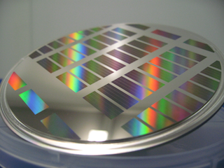
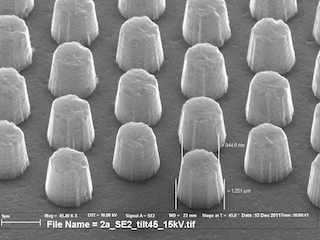
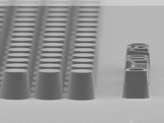
8: Hot-embossing stamp with sub-micron feature arrays
9: Inspection of a hot-embossing stamp with sub-micron feature arrays
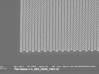
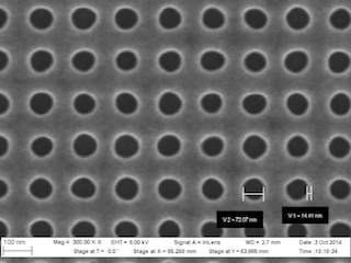
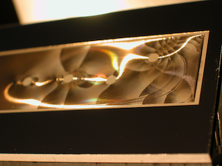
10: SEM-image of sub-micrometer pattern on Nickel-stamp
11: SEM-image of sub-micrometer pattern on Nickel-stamp
12: Hot-embossing stamp with 200nm feature size arrays (PHABLE)
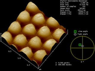
13: AFM plot on nanopatterned Nickel-stamp
14: SEM-image of 70nm dot-array on a Nickel-stamp (SEM courtesy of Eulitha AG)
15: Set of hot-embossing stamps fully covered with cylindric lenses
16: Close-up on hot-embossing stamps fully covered with cylindric lenses
17: Hot-embossing stamp with regular grating pattern to fit Jenoptik-HEX machine
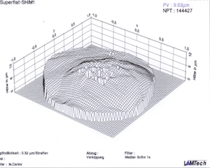
18: Surface-scan (White-light interferometry) of Ni/steel-hybrid injection mold.
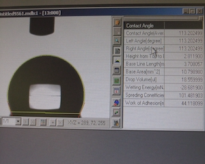
19: Contact-angle analysis after surface-treatment with anti-sticking coating on Ni-stamp.
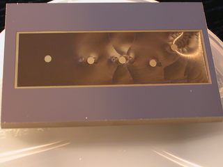
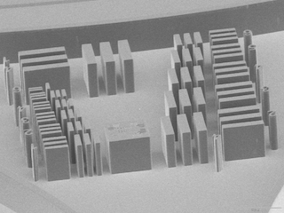
20: Hot-embossing stamp with complex microfluidic layout
21: Hot-embossing stamp with complex microfluidic layout
22: Hot-embossing stamp with cylindrical lens-arrays
23: Hot-embossing stamp with cylindrical lens-arrays
24: Set of hot-embossing stamp with cylindrical lens-arrays
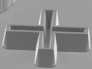
25: SEM-image of photoresist-feature with drafted sidewalls (Height = 250µm)
26: SEM-image of photoresist-pattern with drafted sidewalls
27: SEM-image of USAF test-pattern (photoresist) with vertical sidewalls
Material: PDMS (silicone) soft stamp, silicon wafer, EF-Nickel or Steel-stamps
Applications: nano- and microoptics, microfluidics.
1. Convert customer data into Maskdesign
2. Fabrication of maskset
3. Lithography on substrates =» resist-master
4. Prepare the master for Ni-electroforming =» Nickel-master (pattern inverted / mirrored)
5. Removal of wafer and resist
6. Mechanical post-processing the geometry of the stamp for mounting on the hot-embossing machine.
1. Prepare the customer-substrate for Ni-electroforming =» Nickel-master
2. Removal of wafer and resist
3. Mechanical post-processing of the stamp geometry for mounting on the hot-embossing machine.
Specifications:
- Pattern depth range = 70nm - 500μm
- Pattern height uniformity = 3 – 5%
- EXCLUSIVE: Adjustable drafted sidewalls up to 15° (easy demolding)
- Manufacturing according to adapted LiGA-process
- Multilevel pattern available (micro+nano)
- Alignment-precision: level-to-level ≤ 3μm
- Alignment-precision: micropattern to machined features ≤ 20μm
- Stamp thickness = 0.5 - 3mm
- Maximal stamp dimensions = 300 x 300mm
- Maximal patterned area = 200 x 200mm
- Parallelism Frontside-to-backside ≤ 20μm (Backside: surface grinded)
- Robust handling
- Integration of mechanical mounting features
- Ready-to-use stamps according to customer drawing
- Contour wire-electrodischarge machined (tolerance = ± 10µm)
- Available antisticking-coating (fluoro-based)
- Available wear-protection coating (TiN)
- Compatibility to most patterning methods: - e-beam resists (PMMA, HSQ)
- XIL-resists
- UV-lithography: AZ positive resists, Microchem SU-8
- Hot-embossed polymers, Thermal imprinting,...